
qSlot
In the field, industrial IoT systems (especially smart agriculture, where maintenance windows are tight and failure costs are high) tend to accumulate the same fundamental problem: as functions grow, wiring, interface variety, and service processes become hard to manage. On a carrier board, different communication modules (GSM/LTE, LoRa, Wi‑Fi), sensor interfaces, IO expansions and power converters are co-located; every new need often triggers a new motherboard revision, more manual service on site, and longer troubleshooting.
qSlot aims to reduce this complexity with one principle: instead of permanent cable harnesses and single-purpose motherboards, functions are managed through a standard plug‑in module slot. This allows fast service by swapping modules on site; new functions can be added at module level using the same mechanical and electrical interface; as the platform grows, both production and maintenance remain predictable and scalable.
qSlot is intended to be an open-source ecosystem, enabling third parties to develop modules with the same physical/electrical interface.
What it is and what it is not
qSlot is a slot standard defined to provide modularity in the field. “Standard” here does not mean universal compatibility where any module fits any slot. It defines a controlled ecosystem within a specific system architecture, where each slot’s role and the class of modules it accepts are predefined.
Slots are not "general-purpose". For example, a communication slot is designed to accept only GSM/LTE, LoRa or Wi‑Fi/BLE modules; its power levels (e.g., VCC class), enable signals and expected interfaces are fixed to that role. This prevents wrong module-slot matches, ambiguous power expectations and service-time mistakes.
qSlot’s relationship with PCIe is mechanical only. It uses the PCIe Mini Card connector and form factor for availability, mature ecosystem and robust mechanical latching. qSlot does not implement the PCIe protocol—no PCIe lane mapping, enumeration or device compatibility. Instead, this document defines a custom pin map on the connector and provides a modular electrical interface for power, control and common peripherals (I2C/SPI/UART etc.).
The qSlot connector may look like Mini PCIe; however, PCIe devices (e.g., a Mini PCIe Wi‑Fi card) will not work in qSlot. qSlot is only compatible with the pin map and slot classes defined by this specification.
Scope
This document provides the normative technical definition of qSlot v1.0—i.e., the minimum rules and boundaries for carrier and module designs to interoperate. The focus is not “what each module does,” but how the common interface is structured so modules can be reliably hot-plugged and serviced in the field.
It covers how the PCIe Mini Card form is used within qSlot, socket choice and mechanical height constraints, the pin map and pin function classes (power, control, communication, analog/digital IO). It also explains usage of power rails (3V3/VCC/POWER_FEED), enable signal behavior (PWR_EN and COMM_EN), domain rules and minimal ESD/EMI and backfeed prevention practices for reproducible designs.
Out of scope are the layers built on top of the interface: individual module schematics/BOMs, the carrier’s system architecture (CPU choice, power topology, backplane layout), and software/firmware drivers or upper protocol agreements. These must be defined in separate module docs and platform documentation referencing qSlot.
Terms like MUST / MUST NOT / SHOULD / MAY denote mandatory or recommended rules for compliance. Application documents may extend these but must not restrict in ways that break qSlot v1.0 compatibility.
Terms and abbreviations
- qSlot: Modular slot standard that uses PCIe Mini Card mechanics but the electrical pin map and behaviors defined in this document.
- Mini Card / Mini PCIe: The connector and card form family qSlot leverages mechanically.
- Carrier: The main board hosting one or more qSlot slots and providing platform power/CPU/base interfaces.
- Module: A plug-in function card that fits into a qSlot slot and is intended for hot-swap operation.
- Slot: A single qSlot connector position on the carrier.
- Slot class: Classification that fixes a slot’s role and key parameters (especially VCC level), enforcing correct module-slot matching.
- Domain: Voltage domain against which level definitions are referenced (e.g., 3V3 domain). Digital interface levels are evaluated by domain.
- Enable signal: Control line to enable/disable a function. qSlot defines PWR_EN and COMM_EN.
- Hot‑plug: Insertion/removal while the system is powered. qSlot includes rules to mitigate backfeed and bus instability.
- Backfeed: Unwanted powering of carrier rails (3V3/VCC) from a module.
“MUST / MUST NOT / SHOULD / MAY” in this document denote compliance-critical or recommended rules.
Card size standards
qSlot leverages the mature manufacturing ecosystem of PCIe Mini Card on the mechanical side. Card sizes and mounting directions follow common Mini Card practices. The goal is a single “mechanical language” for module designers and predictable slot placement/service decisions on carriers.
Four basic forms are defined: Full/Half length, each with Single/Double assembly options. "Single/Double" does not imply electrical differences; it only refers to single-sided or double-sided component placement.
| Standard | Card Name | Description | Size |
|---|---|---|---|
| F1 | Full Mini Double | double-sided assembly | 50.95 x 30 mm |
| F2 | Full Mini Single | single-sided assembly | 50.95 x 30 mm |
| H1 | Half Mini Double | double-sided assembly | 26.80 x 30 mm |
| H2 | Half Mini Single | single-sided assembly | 26.80 x 30 mm |
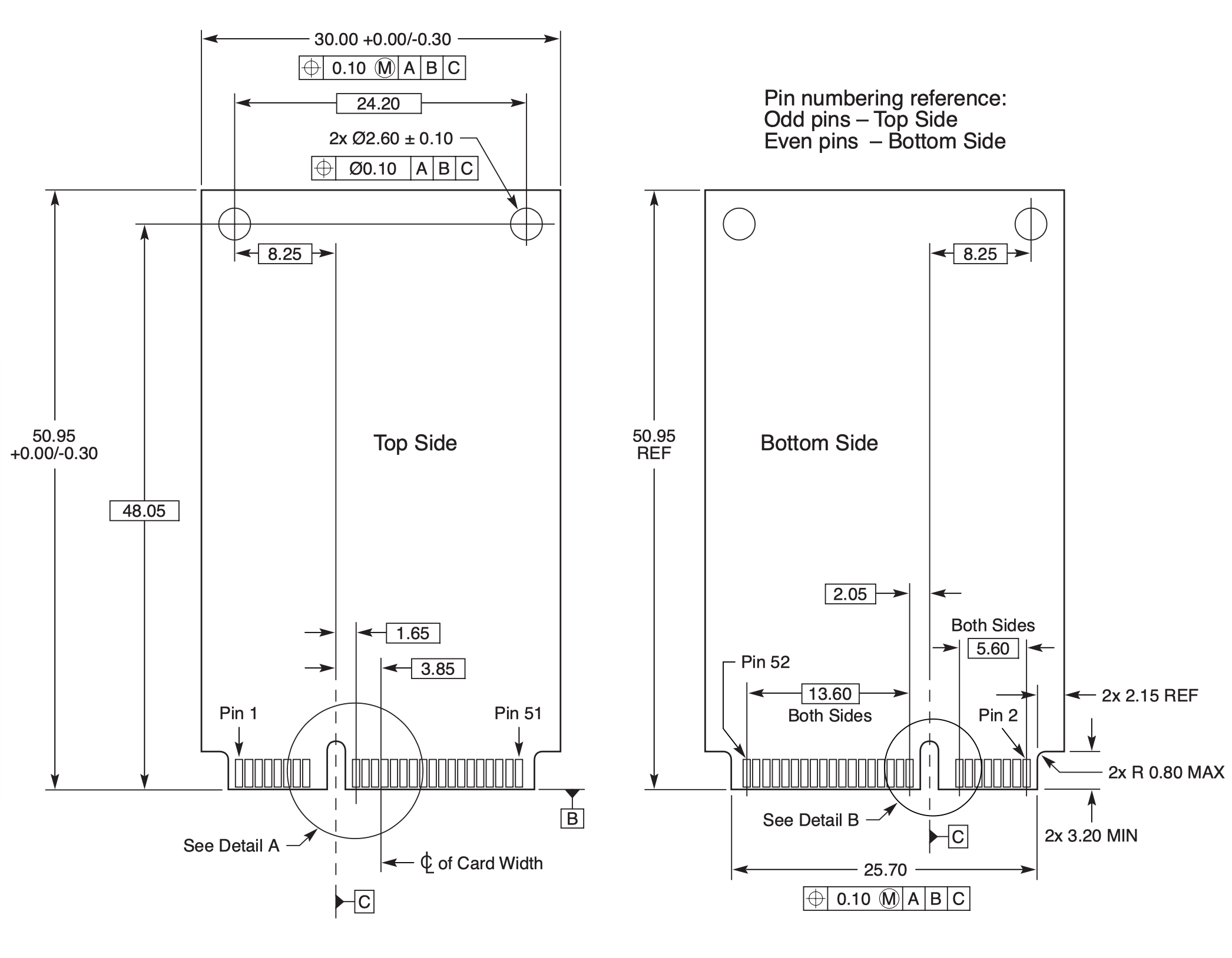
Given target field robustness and component variety, modules are practically designed as double-sided and carried by taller Mini Card sockets. Single-sided should only be chosen when mechanical height or manufacturing constraints require it.
Connector and mechanical constraints
qSlot uses the key geometry of the Mini Card family, structurally preventing incorrect insertion. Yet field reliability is mostly determined by board-to-board clearance implied by socket choice and corresponding component height envelope. Thus, when selecting the socket family on the carrier, the maximum component heights on module faces must be set as early design inputs.
As a reference, with TE Connectivity 1775862‑2 socket, the max component height allowed on the module bottom face is 1.35 mm. This yields about 1.45 mm free clearance and a typical ~2.8 mm board-to-board spacing. These values must be treated as design inputs for footprint selection, placement and tolerance analysis.
If a module needs tall components on the bottom, a standard socket may be insufficient. Choose a taller socket family or steer the module to single-sided assembly; otherwise vibration and tolerance stacking can increase contact risk.
Pin map (qSlot v1.0)
This section defines the physical positions of pins on the qSlot connector and assigns them to functional classes. The pin map is the primary reference for interoperable module/carrier designs.
Electrical limits, default states, pull-up/down recommendations, ESD/EMI measures are expanded in related sections or dedicated Pin Description pages. The table below fixes locations and naming.
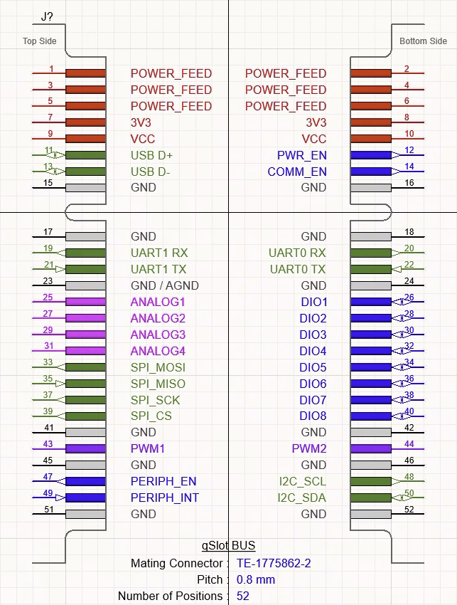
Show pin position table (text)
| Top Side | Pin ID | Pin ID | Bottom Side |
|---|---|---|---|
| POWER_FEED | 01 | 02 | POWER_FEED |
| POWER_FEED | 03 | 04 | POWER_FEED |
| POWER_FEED | 05 | 06 | POWER_FEED |
| 3V3 | 07 | 08 | 3V3 |
| VCC | 09 | 10 | VCC |
| USB_D+ | 11 | 12 | PWR_EN |
| USB_D- | 13 | 14 | COMM_EN |
| GND | 15 | 16 | GND |
| — | Key | Key | — |
| GND | 17 | 18 | GND |
| UART1_RX | 19 | 20 | UART0_RX |
| UART1_TX | 21 | 22 | UART0_TX |
| GND | 23 | 24 | GND |
| ANALOG1 | 25 | 26 | DIO1 |
| ANALOG2 | 27 | 28 | DIO2 |
| ANALOG3 | 29 | 30 | DIO3 |
| ANALOG4 | 31 | 32 | DIO4 |
| SPI_MOSI | 33 | 34 | DIO5 |
| SPI_MISO | 35 | 36 | DIO6 |
| SPI_SCK | 37 | 38 | DIO7 |
| SPI_CS | 39 | 40 | DIO8 |
| GND | 41 | 42 | GND |
| PWM1 | 43 | 44 | PWM2 |
| GND | 45 | 46 | GND |
| PERIPH_EN | 47 | 48 | I2C_SCL |
| PERIPH_INT | 49 | 50 | I2C_SDA |
| GND | 51 | 52 | GND |
Pin segments and functional classes
Pins are segmented to improve readability and clarify "which signal serves which purpose" in module designs. Segments encode both functional roles and expected design practices.
Power distribution
- 3V3: Standard digital domain supply on qSlot.
- VCC: Auxiliary supply fixed per slot class (e.g., 3V8, 5V).
- POWER_FEED: High-current rail using parallel pins for >1A needs.
Design principle: power segment pins must be supported on the carrier by low-impedance distribution and adequate return paths.
Segment short name: PWR
Power and communication control
- PWR_EN: Enables module-side power switching (if present).
- COMM_EN: Enables communication path including buffers/level-shifters.
Design principle: qSlot v1.0 defines these as active HIGH; inverse needs must be handled on the module.
Segment short name: CTRL
Communication channels
- UART0: primary 3V3 UART channel (general purpose).
- UART1: auxiliary UART channel (special domain or second port).
- I2C_SCL / I2C_SDA: master I2C bus (3V3).
- SPI_MOSI / SPI_MISO / SPI_SCK / SPI_CS: 3V3 SPI bus.
- USB_D+ / USB_D-: optional service/test USB data lines.
Design principle: I2C modules MUST use a buffer; SPI_CS is solely for chip-select.
Segment short name: COMM
Analog measurement lines
- ANALOG1..4: Analog lines referenced to 3V3.
Design principle: do not repurpose analog lines as digital IO; route away from noisy regions.
Segment short name: ANALOG
General-purpose IO and PWM
- DIO1..8: 3V3 digital IO lines.
- PWM1..2: 3V3 PWM lines.
Design principle: document IO direction and default states in module docs.
Segment short name: DIO/PWM
Return reference
- GND: Total of 12 pins targeting low-impedance return paths.
Design principle: in high-current paths, place returns close and in parallel; for analog, prefer GND neighbors near analog pins.
Segment short name: GND
Power architecture
qSlot power architecture targets hot-plug capability by (1) making the digital domain predictable across modules and (2) resolving module-specific supply needs via slot class. Three power classes exist: fixed 3V3, slot-class VCC, and POWER_FEED for high current.
3V3
3V3 is the reference domain for all basic digital interfaces (UART0/I2C/SPI/DIO/PWM). Level definitions are fixed to 3V3 to reduce level mismatch risk across modules.
| Property | Value |
|---|---|
| Long Name | DIGITAL_3V3 |
| Short Name | 3V3 |
| Voltage | 3.3 V (fixed) |
| Max Continuous Current | 1 A (two pins total on module) |
3V3 is not meant to carry heavy loads; it stabilizes the digital domain. High-current loads (motor, relay, heater) should use POWER_FEED or VCC.
POWER_FEED
For modules requiring >1A, POWER_FEED is a high-current rail using parallel pins to increase capacity. Voltage level is not fixed by qSlot; it is defined by the carrier and slot class.
| Property | Value |
|---|---|
| Long Name | HIGH_CURRENT_POWER_FEED |
| Short Name | POWER_FEED |
| Voltage | Defined by slot/carrier |
| Max Continuous Current | 3 A (parallel pins total target) |
Actual capacity depends on connector series, contact material, temperature rise, copper width/thickness, vias and return path impedance. Current sharing and thermal analysis on the carrier SHOULD be performed.
VCC
VCC is an auxiliary supply required by module functions (e.g., GSM 3V8, relay 5V). VCC is fixed per slot via slot class, and this must be documented and labeled on the carrier. This reduces damage risk from wrong module-slot matches and ambiguous supply expectations.
| Property | Value |
|---|---|
| Long Name | VCC |
| Short Name | VCC |
| Voltage | Fixed by slot class (e.g., VCC3V8, VCC5V0) |
| Max Continuous Current | 1 A (two pins total on module) |
Each qSlot position on the carrier MUST indicate the VCC level (e.g., VCC=3V8). Slot class info is critical for correct module-slot pairing in the field.
Backfeeding 3V3/VCC from a module to the carrier is undesirable. If the module has local regulators/boost sources, ideal diode/ORing or power switches SHOULD be considered to block reverse paths.
Enable signals (standard behavior)
qSlot defines two enable signals for manageability and energy control: one for power and one for communication. These control module-side switching elements and/or buffers/level-shifters.
Enable logic in qSlot v1.0 is active HIGH. After reset, the carrier should hold these lines in a known state; the module MUST NOT present backfeed or half-enabled behavior when enables are LOW.
| Signal | Purpose | Default logic | Note |
|---|---|---|---|
| PWR_EN | Enables module-side power switching | Active HIGH | With enable=LOW, module loads MUST NOT be powered |
| COMM_EN | Enables communication path | Active HIGH | With enable=LOW, module MUST NOT drive comm lines |
Modules needing active‑low must handle inversion locally. Carrier polarity is not changed, ensuring consistent service behavior across the platform.
UART channels
To manage common communication modules (GSM/LTE, Wi‑Fi/BLE, GNSS, RS‑485 bridges), qSlot defines two UART channels. The intent is flexibility in service/test/integration—not general parallel operation.
UART0 is the primary serial interface and fixed at 3V3. It should be accessible on carriers and referenced as the default port in module docs. UART1 is auxiliary for production test, debug, or different levels, depending on slot class or module design.
| Channel | Role | Voltage domain |
|---|---|---|
| UART0 | Primary serial interface | 3V3 (fixed) |
| UART1 | Auxiliary/test/special | Slot class or module-dependent |
- If a module uses a single UART, UART0 MUST be the default.
- Use UART1 only if justified by platform documentation.
UART lines are named UART0_TX/UART0_RX and UART1_TX/UART1_RX. Do not use alternative abbreviations in schematics/PCB symbols.
Master I2C bus
qSlot defines a single master I2C backbone from the carrier to modules—good for low-speed, multi-peripheral and serviceable designs like sensors, IO expanders and measurement ICs. It runs at 3V3 and is physically shared, requiring precautions for address conflicts and hot-plug/power switching.
Therefore, modules using I2C MUST include an I2C buffer for isolation and re-drive. The buffer prevents dangling buses when a module is absent, reduces backfeed when unpowered, and allows address/segment management in multi-module systems.
| Property | Value |
|---|---|
| Lines | I2C_SCL, I2C_SDA |
| Voltage | 3V3 |
| Topology | Shared master bus |
| Direction | Bidirectional |
Pull-ups and total bus capacitance must be managed at platform level. Do not multiply pull-ups by letting each module add its own.
PERIPH_EN and PERIPH_INT
Two peripheral control lines are defined, not limited to I2C use:
- PERIPH_EN (3V3): Enable line for a specific on-module peripheral (sensor, IO expander, measurement IC).
- PERIPH_INT (3V3): Interrupt/notification from the peripheral to the carrier.
These can be used beyond I2C; module docs must state which component they control and the default behavior.
Naming these as I2C-only would constrain SPI/UART topologies. PERIPH_EN/PERIPH_INT represent a neutral peripheral control interface.
SPI bus
For higher speed and deterministic timing, qSlot provides a 3V3 SPI interface, useful for ADC/DAC, fast IO expanders, external memories, and some RF peripherals.
- SPI_MOSI: master → slave data
- SPI_MISO: slave → master data
- SPI_SCK: clock
- SPI_CS: chip-select (active LOW convention must be documented by the module)
SPI_CSis solely for chip-select; do not reuse as RESET/ICSP.- In multi-module scenarios, each module must use its own chip-select; do not share CS.
- Level translation needs (1V8 etc.) must be solved on the module; the platform domain is fixed at 3V3.
Analog lines (ANALOG1..4)
To expose carrier ADC resources to modules, qSlot defines 4 analog lines for sensor outputs, referenced measurements or low-bandwidth analog signals. These are not repurposed as digital IO; routing/filters assume analog usage platform-wide.
Analog lines are referenced to 3V3. Actual measurement range (e.g., 0–3.3V), ADC reference design and input filtering are defined by the carrier/platform docs. The module must match this interface for output range, source impedance and protective elements.
| Property | Value |
|---|---|
| Lines | ANALOG1..4 |
| Reference | 3V3 domain |
| Usage | sensor analog output / low-speed analog measurement |
- Modules MUST apply only analog levels to ANALOG lines; do not use PWM/1‑wire/bit‑bang.
- Module analog outputs must tolerate input filter and ADC sampling currents; consider buffer/RC conditioning for high source impedance sensors.
- Carriers should add input protection (ESD, reasonable over-voltage clamp). Modules near field cabling may add extra protection MAY.
Route analog lines short and shielded, away from high-current/noisy paths. Avoid POWER_FEED/VCC switching regions, RF lines and fast-edge digital lines; prefer GND neighbors near analog pins.
Digital IO lines (DIO1..DIO8)
For module-level control/IO needs, qSlot defines 8 digital IO lines at 3V3. They serve relay driving, status reads, basic control signals and low/medium-speed digital interfaces.
If a module needs more than 8 IOs, prefer I2C IO expanders (or similar) instead of expanding the connector pin map. This keeps backward compatibility while allowing flexible IO scaling at module level.
| Property | Value |
|---|---|
| Lines | DIO1..DIO8 |
| Voltage | 3V3 |
| Direction | input/output (module-dependent) |
PWM lines (PWM1..PWM2)
Two PWM lines serve timing and duty-cycle control needs (fans, LED dimming, simple motor/valve control, pulse generation or direct access to carrier timers).
PWM count is intentionally two—to cover common needs without growing the pin map. If a module needs more than two, use local generation (small MCU/FPGA) or I2C PWM drivers/expanders.
PWM frequency range, resolution and default duty depend on carrier timer design. Modules must conform to platform-defined limits and document expected ranges.
| Property | Value |
|---|---|
| Lines | PWM1, PWM2 |
| Voltage | 3V3 |
| Direction | input/output (module-dependent) |
Ground (GND)
GND is a single domain, the common reference. This avoids fragmentation of references during hot-plugging, keeps return currents predictable and improves tolerance to service/layout mistakes.
There are 12 GND pins targeting a total return capacity of 6 A. Real capacity depends on GND plane continuity, via density, copper distribution near the connector and return paths near power lines.
qSlot v1.0 does not define a separate AGND domain. If needed, pin 23 MAY be reserved as AGND. If used this way, it MUST be declared in the module docs.
USB
USB_D+ / USB_D− are defined strictly as service/test data lines. Since USB host/device roles and connector topology vary per platform, qSlot does not make assumptions about USB power; only the differential pair interface is fixed.
On platforms using USB, ensure ESD protection and differential routing rules (length matching, controlled impedance, continuous reference planes) per platform design rules.
If USB is used, do not reinterpret VCC as USB VBUS. Use an explicitly managed USB_VBUS_5V. qSlot’s VCC is the auxiliary supply fixed by slot class and must not be confused with USB VBUS.
Design rules
Minimum design rules to preserve qSlot v1.0 compatibility for both carriers and modules, aiming to reduce common field failure classes (ESD damage, EMI instability, backfeed and mis-powering).
ESD and field robustness
Because qSlot may expose signals to field cabling/user interaction, ESD robustness is part of compliance. Evaluate ESD protection for every line extending to the outside world (UART/I2C/SPI/DIO/PWM). Placement matters: ESD components should be as close to the connector entry as possible, with short return paths.
The carrier should act as the primary protection layer for lines exiting qSlot. Modules near field cabling or with analog sources may add extra protection where needed.
EMI and routing
Power and signals share the connector; routing rules are critical for stability and measurement accuracy. Carry POWER_FEED/VCC with wide copper and provide low-impedance GND returns. Keep ANALOG lines away from power switching, RF regions and fast-edge digital lines.
For I2C: manage pull-ups and bus capacitance at platform level; prevent modules from adding uncontrolled pull-ups. Buffer requirement serves address/segment management and keeps bus load under control.
Backfeed prevention
In hot-swap modular systems, module-side regulators/boost sources may unintentionally backfeed 3V3 or VCC. If backfeed is undesired by the platform, use ideal diode/ORing or appropriate power switch topologies on the module. Combine with the “enable=LOW → do not drive” rule on carriers to avoid half-enabled states.
Do not carry mains (110/220VAC) through the qSlot connector. High-voltage measurement/power modules must take mains via separate terminals/connectors; qSlot should only carry isolated low voltages and control signals.
Versioning and backward compatibility
Across qSlot v1.x, the primary goal is to grow the ecosystem while preserving backward compatibility. Therefore, pin map, domain rules and normative behaviors (enable logic, I2C buffer requirement) MUST NOT change in breaking ways within v1.x.
When new needs emerge, prioritize non-breaking extensions: use reserved areas, carry a function over an existing interface, or employ expanders/aggregators on the module. Pin meaning or electrical assumptions requiring breaking changes should be reserved for v2.0.
Bu kütüphane, gerçek sahada kullanılan projelerden gelen ihtiyaçlara göre sürekli gelişen bir açık kaynak projedir. Kullanıcı geri bildirimleri, yeni fonksiyonların eklenmesi ve mevcut yapının iyileştirilmesi açısından kritik öneme sahiptir.
Bu kütüphaneyi hem kişisel hem de ticari projelerinde özgürce kullanabilirsin. Herhangi bir lisans kısıtı uygulanmamaktadır; amacım, bu kütüphanenin mümkün olduğunca fazla gerçek dünya projesinde yer almasıdır. Özel bir entegrasyon ihtiyacın, ticari bir planın veya teknik bir sorunun varsa bana e‑posta üzerinden her zaman ulaşabilirsin: akkoyun@me.com Geri bildirimlerini veya kullanım senaryolarını paylaşman, projeyi geliştirmem açısından büyük katkı sağlar.